薄膜トランジスタ(TFT)/ Thin-film Transistors (TFT)
フレキシブルディスプレイ実現に向けた酸化物半導体薄膜トランジスタの高性能化に関する研究を行っています。真空成膜および溶液成膜の2つの手法を活用し、低温プロセスで高性能な素子実現を目指します。
●溶液法を用いたゲート絶縁膜,保護膜の高性能化
●イオントロニクスによる高信頼性、低駆動電圧IGZO TFTの開発
●溶液,真空プロセスで作製したHigh-k薄膜による酸化物TFT高性能化
●酸化物半導体の電気伝導率制御によるセルフアラインプロセスの開発
We are conducting research on enhancing the performance of oxide semiconductor thin film transistor for the realization of flexible displays. By utilizing two deposition methods: vacuum and solution process deposition, we aim to achieve a high performance using low temperature processes.
● High performance solution processed gate insulators and passivation layers
●Development of highly reliable, low voltage driven IGZO TFT by iontronics
● Improvement of oxide TFT using High-k dielectric thin films prepared by solution and vacuum process
●Development of a self-aligned process by selectively controlling electrical conductivity of oxide semiconductors
Transparent oxide semiconductor TFT
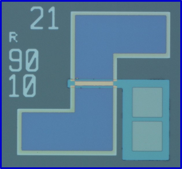
Micrograph of TFT structure
熱電変換素子/ Thermoelectric conversion element
熱電変換素子は体温など身の回りの廃熱から直接電力を生み出すことが可能なため、材料や構造の革新により性能向上ができれば身近な電力源としての利用が期待できます。 私たちは、低い熱伝導率をもつアモルファス材料に着目しています。特にフレキシブル基板に成膜できる透明なアモルファス酸化物半導体を用いて高性能化を目指した研究をしています。 また、ナノ構造を形成することで熱伝導率を低減させ、性能向上を目指した研究も行っています。
Because thermoelectric conversion elements can generate electric power directly from waste heat such as body heat and ambient heat, by improving the material performance through innovation of its properties and structure, we can expect these to be used as an ubiquitous power source. Currently, we focus on amorphous materials with low thermal conductivity. We are aiming to achieve a high performance using transparent amorphous oxide semiconductors which can be deposited on flexible substrates. We are also aiming at improving performance by reducing the thermal conductivity through the formation of nanostructures.
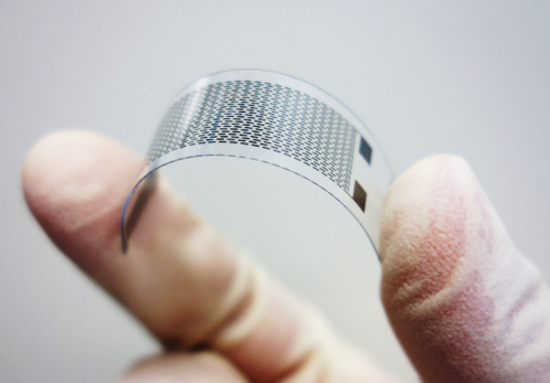
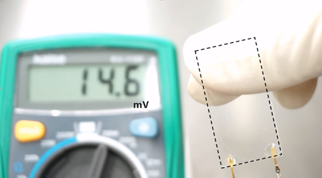
Flexible thermoelectric element
Transparent thermoelectric element
太陽電池/ Solar Cells
本研究グループでは、屋外・屋内用途それぞれに対しての光電変換素子開発および測定技術の開発を行っています。現在は以下のトピックに注力して研究を行っています。
(1) 結晶シリコン太陽電池の更なる低コスト作製手法の開発
(2) エレクトロルミネッセンス(EL)法などによる太陽電池劣化早期発見技術の開発
(3) FeS2パイライトを用いた光電変換素子の開発
(4) 低照度用途に向けたペロブスカイト型太陽電池の開発
In this research group, we are developing photoelectric conversion elements and characterization techniques for both outdoor and indoor applications. Currently, we focus and conduct research on the following topics.
(1) Development of extra low cost fabrication methods for crystalline silicon solar cells
(2) Development of technology for early detection of solar cell degradation through an electroluminescence (EL) method
(3) Development of photoelectric conversion device using FeS2 pyrite
(4) Development of perovskite type solar cells for low light intensity applications
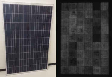
Analysis of degradation by EL Emission
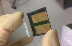
Perovskite Solar cell
パワーエレクトロニクス/ Power Electronics
省エネルギー化の観点として、インバータ等の電力変換のキーコンポーネントであるパワーデバイスの低損失化が求められています。 パワーデバイス用途の半導体材料としては窒化物半導体であるGaN(窒化ガリウム)が注目されており、 現在主流であるSi(シリコン)パワーデバイスの限界を超えた高効率・低損失デバイスの実現への期待が高まっています。 次世代GaNパワーデバイスの開発は、現在非常に勢いのある研究です。私たちは金属-絶縁体-半導体の層構造をしたMOS構造において、 酸化膜成膜プロセスやアニールプロセスに着目し特性改善の推進と基礎物性評価に取り組んでいます。
From an energy conservation viewpoint, low power loss from power devices which are key components of power conversion of inverters etc. is required. GaN (gallium nitride), which is a nitride semiconductor, is attracting attention as a semiconductor material for power device applications. With GaN, realization of high efficiency / low loss device exceeding the limit of currently used Si (silicon) power device is rising. The development of next-generation GaN power devices is currently a very significant research. We focus on the oxide film deposition process and annealing process in the MOS structure with the metal-insulator-semiconductor layer structure. We are also promoting the improvement of characteristics and the evaluation of basic physical properties.
2 in. GaN wafer
High Pressure Water Vapor Annealing